


HBM 4, the battle begins!
Currently, HBM chips account for 15% of the general memory market, compared to 8% last year. Around HBM, manufacturers are also coming up with various strategies. In addition to deepening their efforts on existing technologies, they are quietly sounding the horn of attack around the future HBM 4
The heat of AI has not only driven the popularity of GPUs, but also put the important storage technology HBM in the spotlight in recent years. Recently, the performance and actions of SK hynix and Samsung indicate a promising future for HBM.
According to Reuters, HBM chips currently account for 15% of the general memory market, up from 8% last year. SK hynix has the largest market share in the HBM market, with the demand for Nvidia GPUs stimulated by the generative AI trend leading to a sharp increase in demand in this market. It is the sole supplier of HBM3 memory for Nvidia, which holds an 80% share of the AI GPU market, and began mass production of the latest generation HBM3E in March. Competing suppliers like Micron and Samsung are developing their own HBM products to prevent SK hynix from dominating the market.
Around HBM, manufacturers are also coming up with various strategies. In addition to deepening their efforts on existing technologies and focusing on future HBM 4, they are quietly sounding the horn for an offensive (for more information on HBM4, please refer to the article "HBM4 is Coming"). Additionally, it should be noted that because the author did not find more information about Micron's HBM technology, this article does not discuss their prospects and insights into HBM technology, so we hope everyone can provide additional information.
SK hynix Adheres to MR-MUF
According to SK hynix, packaging technology has surpassed its traditional role of "electrically connecting chips and protecting them from external impacts" to become an important technology for achieving differentiated product performance. SK hynix's HBM has won outstanding market reputation with its core technologies of Through Silicon Via (TSV) and Mass Reflow-Molded Underfill (MR-MUF) advanced packaging processes.
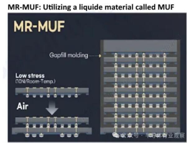
Among them, TSV technology is common, and in MR-MUF, mass reflow soldering (MR) is a technology that connects chips to each other by melting protrusions between stacked chips. Molded underfill (MUF) is a technology that fills protective material between stacked chips to improve durability and heat dissipation Using MR-MUF, multiple layers of DRAM can be encapsulated at the same time.
Specifically, from a technical process perspective, underneath the DRAM, there are lead-based "bumps" connecting the chips. The MR technology involves heating and simultaneously melting all these bumps for soldering. After connecting all the DRAM, the next step is a process called MUF to protect the chips. Epoxy sealant known for excellent heat dissipation is injected to fill the gaps between the chips and encapsulate them. The components are then hardened through heating and pressure to complete HBM.
SK hynix describes this process as "applying heat uniformly like baking in an oven, bonding all chips at once to make them stable and efficient."
In a recent blog post, SK hynix executives stated that to meet the demands of the AI era, SK hynix is focusing on developing 'iconic memory products' to meet customers' differentiated needs in terms of performance, functionality, size, form, and efficiency. To achieve this goal, the company is advancing the development of TSV and MR-MUF technologies, which play a crucial role in HBM performance.
It is worth mentioning that, although MR-MUF is widely used, it must be acknowledged that MR-MUF has drawbacks such as susceptibility to warping, causing wafer end bending, and void phenomena (uneven distribution of protective material in certain areas), which can negatively impact the reliability of MR-MUF. However, SK hynix stated that compared to the early stages of HBM development, they have successfully reduced warping and are currently developing technologies to overcome this issue. The next focus will be on reducing gaps.
SK hynix executives emphasize that the company aims to achieve the task of 'beyond HBM packaging technology'. As he mentioned, in the short term, our main goal is to expand production capacity in South Korea to meet the demand in the HBM market, while also maximizing profits by fully utilizing production bases around the world. In the long term, just as MR-MUF technology currently serves as the core process for HBM, ensuring the development of innovative advanced packaging technologies is our goal.
Furthermore, SK hynix is also committed to the development of next-generation advanced packaging technologies such as Chiplets and Hybrid bonding to support heterogeneous integration between semiconductor memory and logic chips, while promoting the development of new semiconductor technologies. Among them, Hybrid bonding is also seen as another new option for HBM packaging. However, unlike previous plans, SK hynix intends to continue using cutting-edge packaging technology MR-MUF in the next generation HBM 4. The introduction of Hybrid bonding technology as an alternative is expected to be slow due to the relaxation of HBM standards At a recent technical conference, SK hynix shared that the next generation packaging technology is moving towards the direction of integrating memory, logic, and controllers, such as 2.5D. SK hynix is also using these technologies to make HBM more robust.
When discussing the future of HBM, SK hynix believes that the market will lean towards specialized and customized products to meet customer needs. They emphasize that for the new generation of HBM, outstanding performance is a basic requirement, while also needing to have advantages that surpass traditional memory performance to meet specific customer needs.
In addition, SK hynix previously signed a Memorandum of Understanding (MoU) with TSMC to collaborate on developing the next generation of HBM and enhancing logic and HBM integration through advanced packaging technology.
The company plans to continue developing HBM4, the sixth generation product in the HBM series, with mass production expected to begin in 2026.
SK hynix stated that the collaboration between the global leader in AI storage and TSMC will bring more innovation to HBM technology. This collaboration is also expected to achieve breakthroughs in memory performance through tripartite cooperation between product design, foundries, and memory providers.
The two companies will initially focus on improving the performance of the base chips installed at the bottom of the HBM package. The manufacturing method of HBM involves stacking core DRAM chips on top of base chips using Through Silicon Via (TSV) technology and vertically connecting a fixed number of layers in the DRAM stack to the core chip with TSV to form the HBM package. The base chip at the bottom is connected to the GPU controlling the HBM.
SK hynix has used proprietary technology to manufacture base chips up to HBM3E, but plans to adopt TSMC's advanced logic process on the HBM4 base chip to encapsulate additional functions in limited space. This will also help SK hynix produce customized HBMs to meet a wide range of customer demands for performance and efficiency.
SK hynix and TSMC have also agreed to collaborate on optimizing the integration of SK hynix's HBM and TSMC's CoWoS (Chip on Wafer on Substrate) technology, while jointly addressing common customer requirements related to HBM.
SK hynix's President and Head of AI Infrastructure, Justin Kim, said, "We hope to establish a strong partnership with TSMC to accelerate our open collaboration with customers and develop the best performing HBM4 in the industry." "Through this collaboration, we will further strengthen our market-leading position as a provider of overall AI memory by enhancing competitiveness in the customized memory platform area." "Over the years, TSMC and SK Hynix have established a strong partnership. We work together to integrate the most advanced logic and cutting-edge HBM to provide world-leading AI solutions," said Kevin Zhang from TSMC. "Looking ahead to the next generation HBM4, we believe that we will continue to collaborate closely to offer the best integrated solutions and drive new AI innovations for our mutual customers."
Samsung Considers Hybrid Bonding
Unlike SK Hynix, Samsung uses TC-NCF (thermal compression with non-conductive film) in HBM packaging, which is a non-conductive film thermal compression.
Technically, this is a slightly different technology from MR-MUF. Each time chips are stacked, a non-conductive adhesive film is placed between each layer. This film is a polymer material used to insulate the chips from each other and protect the interconnects from impact. As development progresses, Samsung has gradually reduced the thickness of the NCF material, reducing the thickness of the 12-layer fifth-generation HBM3E to 7 micrometers (μm). The company stated, "The advantage of this approach is to minimize the potential warping that may occur with increasing layers and decreasing chip thickness, making it more suitable for building higher stacks."
According to Samsung, the TC NCF method has advantages in stacking higher layers. However, for this technology, optimizing heat and pressure are key to its success. Therefore, it is reported that Samsung has been in discussions with equipment manufacturers to further enhance its innovation. Facing competition from SK Hynix, Samsung Electronics announced "Advanced TC-NCF" technology in February, focusing company-wide efforts on this. This technology can reduce the thickness of the necessary film in the TC-NCF process, thereby increasing the number of semiconductor layers while maintaining the height of HBM.
In addition, there are reports that Samsung's TC NCF yield is not as good as SK Hynix's, so Samsung Electronics is considering introducing MUF material into the through-silicon via (TSV) process. Reports indicate that Samsung has also purchased hardening (forming) equipment from Japan to make this MUF material rigid. It is worth noting that SK Hynix used NCF before the second generation HBM, but switched to MUF (especially MR-MUF) from the third generation (HBM2E) onwards. Analysts believe that MUF is the reason why SK Hynix stands out in the HBM market, which is why there are reports that Samsung is also seeking to develop and introduce this technology. A semiconductor industry executive familiar with Samsung's situation stated, "From what I understand, the MUF material Samsung is researching is not exactly the same as SK Hynix's technology." Afterwards, Samsung denied this and emphasized that the company will continue to focus on TC NCF. In a recent blog post, Samsung shared their views on the future.
When asked why the company's current HBM is so unique, Samsung emphasized that the company's insights into Advanced TC NCF are indispensable. Samsung further stated that HBM uses vertical stacking of DRAM chips (such as 8H and 12H) to increase capacity and bandwidth. However, different generations of HBM all follow a predetermined overall thickness. Under this constraint, as additional layers are stacked, the core bare die responsible for data storage inevitably becomes thinner, which may pose challenges to assembly, leading to chip warping or cracking, as well as increased thermal resistance.
According to Samsung, the thermal resistance of HBM is mainly affected by the chip spacing, and Samsung possesses advanced high-density stacked chip control technology to reduce the thickness of NCF material between chips, and uses thermal compression technology to make the chips more compact. This innovative approach achieves the industry's smallest 7 micrometer (um) chip spacing. Additionally, in the chip bonding process, Samsung strategically designs small bumps for signal transmission and large bumps crucial for heat dissipation. This optimization enhances heat dissipation and yield. Furthermore, by minimizing the size of individual DRAM chips within limited packaging dimensions using process technology, Samsung ensures outstanding mass production capabilities and reliability, providing a significant competitive advantage.
Samsung also mentioned that the industry is increasingly realizing that isolated efforts by processor and memory companies to optimize their products are insufficient to unleash the innovation required for the AGI era. Therefore, "customized HBM" has become a trend, representing the first step towards achieving synergistic optimization between processors and memory to accelerate this trend. To this end, Samsung leverages its comprehensive capabilities in memory, foundry, system LSI, and advanced packaging. Additionally, Samsung has established a dedicated team for the next generation of HBM, utilizing the company's unparalleled capabilities, as we are committed to making significant changes in shaping the future.
Regarding future plans, Samsung stated that the HBM market is still in its early stages and is expected to undergo rapid changes. The company's strategy is to maintain a leading position by predicting market developments and proactively planning and developing necessary products in advance. As the HBM market matures, Samsung expects three major changes to reshape the industry:
Firstly, "segmentation". In the early stages of HBM, hardware needed to be multifunctional. However, as services evolve around killer applications, hardware infrastructure will inevitably be optimized for each specific service. To address this trend, Samsung will provide a range of packaging options (8H, 12H, and 16H) and basic chip variants, while standardizing core chips.
Secondly, achieving a higher degree of customization for synergistic optimization between processors and memory will be necessary. To meet this challenge, Samsung will leverage the creation of platforms to maximize the use of common design elements in HBM solutions and establish an efficient system to meet customization requests by expanding our ecosystem of partnerships Third, in order to overcome the "power wall", the distance between the processor and memory will become closer. The first innovation is evident in HBM4, which adopts logic processing technology in its base chip. The second innovation is the transition from current 2.5D to 3D HBM architecture, and the third innovation involves integrating DRAM units and logic, which is the method for designing HBM-PIM. While actively planning and preparing to lead the market, Samsung has begun discussions with customers and partners to turn these innovations into reality.
Samsung emphasizes that as HBM becomes an undeniable memory solution for generative AI optimization, many customers and data centers are rapidly adopting it. However, ensuring uninterrupted artificial intelligence services is crucial. Even a defective chip could have catastrophic consequences. Therefore, it is imperative to design and test technologies to ensure the quality of HBM. Additionally, developing HBM design structures that can further reduce power consumption and improve system efficiency is also crucial.
To this end, Samsung plans to incorporate 16H technology into the next generation HBM4 through NCF assembly technology optimized for high-temperature environments and cutting-edge process technology. According to Samsung's plan, HBM4 will produce samples in 2025.
However, Samsung Vice President Kim Dae-woo previously stated at a conference in South Korea that Samsung is considering using hybrid bonding or NCF in HBM4 and will begin mass production in 2026. Hybrid bonding is more advantageous as it can compactly add more stacks without the need for silicon through-silicon vias (TSV) using filler blocks for connections. Using the same technology, the core chip DRAM on HBM can also become thicker.
Kim also mentioned that when stacking up to 8 layers, the production efficiency of MR-MUF is higher than TC-NCF, but once the stack reaches 12 layers or more, the latter will have more advantages. The vice president also pointed out that when HBM4 is launched, custom requests are expected to increase. He added that buffer chips will become logic chips, so the chips can come from Samsung or TSMC.
Reports also indicate that NVIDIA will adopt Samsung's technology for HBM packaging, which is another piece of good news for this South Korean giant.
TSMC's Latest Packaging Technology Support
At a technical conference in North America, the company introduced the next-generation wafer-level system platform - CoW-SoW - which will achieve 3D integration with wafer-level design. This technology is built on TSMC's InFO_SoW wafer-level system integration technology launched in 2020, enabling it to build wafer-level logic processors. So far, only Tesla has adopted this technology in its Dojo supercomputer, which TSMC says is now in production.
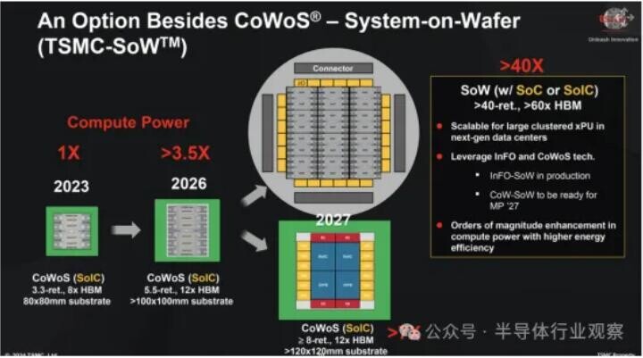 In the upcoming CoW-SoW platform, TSMC will merge two packaging methods in its wafer-level system platform - InFO_SoW and System-on-Integrated-Chip (SoIC). By using Chip-on-Wafer (CoW) technology, this method will be able to stack memory or logic directly on top of the wafer-level system. The new CoW_SoW technology is expected to achieve mass production in 2027, but the actual product launch date is still to be observed.
It is understood that TSMC's CoW-SoW focuses on integrating wafer-level processors with HBM4 memory. These next-generation memory stacks will use a 2048-bit interface, making it possible to directly integrate HBM4 on top of the logic chip. Additionally, stacking additional logic on the wafer-level processor to optimize costs may also be meaningful.
"Therefore, in the future, using wafer-level integration [will allow] our customers to integrate more logic and memory together," said Kevin Zhang, Vice President of Business Development at TSMC. "SoW is no longer a fiction; we have already worked with customers to produce some products that are already in place. We believe that by leveraging our advanced wafer-level integration technology, we can provide customers with very important products that enable them to continue to enhance capabilities, introducing more computing power and more energy-efficient computing for their AI clusters or [supercomputers]."
Generally, wafer-level processors (such as Cerebras' WSE), especially processors based on InFO_SoW, can provide significant performance and efficiency advantages, including high-bandwidth and low-latency core-to-core communication, low-power transmission network impedance, and high energy efficiency. As an additional benefit, such processors also have additional redundancy in the form of "extra" cores.
However, InFO_SoW technology has certain limitations. For example, wafer-level processors manufactured using this method are entirely dependent on on-chip memory, which may not meet the future needs of artificial intelligence (but currently works well). CoW-SoW will address this issue as it will allow HBM4 to be placed on such wafers. In addition, InFO_SoW wafers use single-node processing, which does not support 3D stacking, while CoW-SoW products will support 3D stacking.
Source: [Semiconductor Industry Observation](https://mp.weixin.qq.com/s?__biz=Mzg2NDgzNTQ4MA==&mid=2247736210&idx=1&sn=9c3b4bf6ca363508a80875bcb0b323f5&chksm=ce6e5965f919d07376c007cede27af593c2c58768b635fb0edd58569f49d77aa7367789e06af&mpshare=1&scene=23&srcid=0427G3ZwMgwD8tlDOkh8NP7t&sharer_shareinfo=33bc09c43db63ac08fd9b28a76962d65&sharer_shareinfo_first=33bc0 9c43db63ac08fd9b28a76962d65#rd), original title: "HBM 4, The Battle Begins!"